Tunable LED Lighting Guide: Wattage, Color Temperature & Applications
LED lighting technology has evolved dramatically over the past decade,...
Learn More →Get expert guidance from our Product Specialists who match the right solutions to your project's requirements.

LED lights are currently among the most energy-efficient lighting systems available. Many traditional lighting types are being replaced by LEDs due to their superior energy efficiency, longer lifespan (typically 25,000-50,000 hours), and improved light quality. LEDs emit light when electrons pass through a semiconductor material, making them fundamentally different from traditional lighting technologies.
LEDs are manufactured into various lighting products including fixtures, bulbs, indicator lights, flashlights, and automotive applications. At LED Lighting Supply, we’ve seen how this technology transforms lighting projects across commercial, industrial, and residential applications.
Traditional incandescent lighting creates light by heating a wire filament until it glows. Fluorescent lights use electrical discharge through gas to produce light. Both methods generate significant heat as a byproduct.
LEDs create light through electronic excitation rather than heat generation. This fundamental difference allows LEDs to convert more electrical energy into visible light while producing minimal heat, resulting in greater energy efficiency and longer operational life.
LED lights consist of a small chip with layers of semiconductor material. LED packages contain one or more chips mounted on heat-conducting material known as a heat sink, covered by a lens or optic.
The LEDs are placed on a circuit board that can incorporate lighting controls such as:
The circuit board is positioned on an additional heat sink to regulate LED temperature. Everything is then sealed inside a lighting fixture, architectural structure, or bulb housing.
LEDs use semiconductor diodes made from crystalline material that requires added impurities (dopants) to conduct electricity effectively. These impurities are precisely introduced during manufacturing to create specific electrical properties.
One semiconductor layer has a surplus of electrons (N-type), while the other layer has fewer electrons (P-type). When voltage is applied, electrons move from the N-type layer to the P-type layer through the P-N junction. This electron movement releases energy in the form of visible light through a process called electroluminescence.
Understanding LED manufacturing helps explain why quality varies between products and why professional-grade LEDs offer superior performance and reliability.
Before manufacturing begins, engineers determine these critical LED characteristics:
These specifications are influenced by diode layer thickness, semiconductor materials used, and the types of dopant impurities required. This design phase ensures the final LED product meets specific performance requirements.
Semiconductor wafer production creates the foundation material for LED chips:
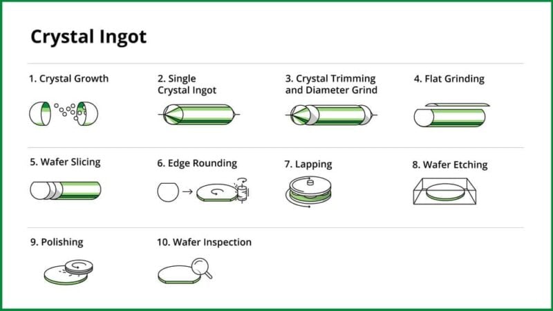
Additional semiconductor crystal layers are grown on the base wafer. During this stage, specific impurities or dopants (typically nitrogen and zinc) are precisely added to create electrical properties.
This process creates two distinct regions:
When voltage is applied, electrons migrate from the N-type to P-type layer through the P-N junction, generating light energy through this controlled electron movement.

Metal contact patterns are applied based on whether the diode will operate individually or as part of an array. The contact metal is deposited using vapor deposition in a high-temperature, vacuum-sealed chamber.
The metal is heated until it vaporizes, then condenses uniformly onto the wafer surface, creating precise electrical connection points essential for reliable LED operation.
Individual diodes are mounted onto their final package assemblies. Fine wire leads connect each diode to the contact metals using specialized bonding techniques. The complete assembly receives a protective coating or encapsulation to ensure long-term reliability.
Advanced processing techniques now enable semiconductor wafer production with unprecedented uniformity and purity. These manufacturing improvements directly impact LED efficiency, brightness consistency, and operational lifespan.
Higher-quality manufacturing processes also allow multiple LED devices to be integrated onto single chips, enabling more sophisticated lighting solutions with better performance characteristics.
When selecting LEDs for professional applications, understanding these manufacturing fundamentals helps ensure you choose products that will deliver reliable, long-term performance for your specific lighting requirements.

Cory Peterson is Vice President of Marketing & Sales Operations at LED Lighting Supply where he focuses on improving customer experience and revenue operations. Cory writes about commercial & industrial lighting, along with topics important to contractors and facility managers. In his free time, Cory enjoys traveling, snorkeling, exercise and cooking.